
 Bad PCB designs are an epidemic now days. Most young engineers either come out of school with no knowledge on good layout practices, or older engineers have bad habits that derive from old manufacturing processes. The consequence of a bad layout are very significant, your design will not be legally sold if it does not pass the appropriate test associated with your industry ( FCC part 15, UL, IEC60601, DO-160, Mil-STD, etc.). Your layout can make the difference in these types of tests. Why does this mater? A bad PCB design can cost you big. It can rack up additional lab fees, consulting costs, and redesign time and materials. In one case, I seen a bad PCB design cost an Aerospace program over $450K. They hired inexperienced designers, and they spent a ton of time in the lab troubleshooting a horrible design. Allow me to brag, Coaction consulting has designed over 150 pcb(s) and each one has passed the testing necessary to launch the product. This is no accident, it has been the result of years of training and experience. So without further ado, here is a small list of do's and don'ts - DO USE ALTIUM DESIGNER, DON'T USE ALLEGRO, EAGLE, OR MENTOR Altium has fantastic tools like 3D board layout (Mechanical CAD generation .iges .step file) that save you tons of money since your mechanical engineer will not have to draw a PCB to fit in his product design. It's like electro-mechanical integration for free. It also has great BOM tools for tracking world wide part inventory and lifetime data. Other CAD packages offer these tools as costly add ons, and it's a general rule of thumb that Altium is offering the bast bang for the buck if you are a system integrator, plus the layout is intuitive. 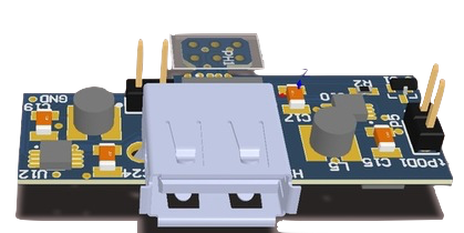 3 D PCB file for mechanical fit check DON'T EVER SPLIT GROUND PLANES AND RUN SIGNAL LINES ACROSS IT If you split your planes, analog on one side and digital on another, then you run a signal across it, you are killing your design. The electrical return path of a signal prefers to always runs directly under a trace, if you split your plane you have created an antenna. Get ready for more noise not less. If you want to keep noisy traces or components from sensitive components, just locate them on opposite ends of the boards. Don't be a fool, although split planes may be intuitive, when you analyse the physics, it is just the opposite. I have seen this mistake cost companies hundreds of thousands of dollars and old engineers big headaches and humbling experiences. Use Dr. W Micheal Kings (the guru) 3W RULE If you want to know how far to place a noisy trace from a sensitive one. Generally it is 3 times the width of the trace. So, if the trace is 10 mils, locate the next trace 30 mils away. Of course, alway place differential pairs as close together as possible. Also, any digital signal with a frequency less that that of RS232 will not be noisy if the ground plane is NOT SPLIT. DON'T PLACE FILTERS OVER GROUND PLANES If you locate a filter (inductor or ferrite bead) under a ground plane, the parasitic capacitance of the PCB board will create an AC short and there will be a diminishing filtering effect. The best practice is to have a ground plane keep out zone under the filter. Also, keep the filters at the board edges right by connectors or shields. Remember, NO SPLIT GROUND PLANES. DO USE LOTS OF VIA TO EQUALIZE THE POTENTIAL LEVELS ON GROUND PLANES Via(s) between plains can keep the noise levels down on your design. Don't worry, it will not cost that much in the manufacturing process and it will be well worth it once you start your certification testing. DO HIRE A COACTION ENGINEER FOR YOUR NEXT LAYOUT Well, this one goes without saying. ;) For more info, follow the link - http://www.coactionconsulting.com/electronic-engineering.html Special Thanks to: http://www.systemsemc.com/ |
AuthorCoaction Staff Writers Archives
August 2017
Categories
All
|
 RSS Feed
How We can Help
|
Project Management
Electronics Product Design Wireless Product Design Printed Circuit Board PCB Layout Printed Circuit Board PCB Fabrication Embedded & Firmware Development Embedded RTOS (Stratify) Industrial Design Mechanical Design FEA Surfacing Internet of Things IoT Website Design Mobile App Development IOS & Android |
Aerospace Engineering
Medical Product Development Consumer electronics Industrial Application Design HIPAA Compliance Network Compliance Testing - IEC60601 - DO160 -Mil Spec 810F Manufacturing ISO6001 AS60001 Mechanical Engineering Electrical Engineering Software Engineering Regulatory Affairs Consulting |

|